5/23/2026 at 5:20:18 PM
The PCB construction is curious (which you say is multi-layer) - why use a grid of 0.1" holes? Is that so it could be easily jumpered? Can you tell if the traces run through the holes or between them?I don't have the patience to reverse-engineer these types of boards, but I do find them really interesting to think about. CAD was just getting started (I just looked up that Gerber format was released in 1980) so I wonder if the masks were hand-drawn.
by GlibMonkeyDeath
5/23/2026 at 7:47:06 PM
The grid is 0.1" holes because that's the spacing of most components; it's a bit like perfboard. If you're asking why they used a grid instead of a normal-style PCB, I'm not sure. It probably makes manufacturing the boards much easier since you can drill the holes with an assembly line rather than one at a time. The traces go between the holes; the traces are very narrow, so two traces can fit between a pair of holes. That's probably the tradeoff, that your traces need to be very precise and you probably need more layers because of all the holes in the way. The layout was probably done with CAD; PCBs with CAD go way back. IBM was doing circuit boards with CAD back in the early 1960s, using a flying spot of light to draw out the PCBs on photoresist.by kens
5/23/2026 at 10:41:19 PM
>The traces go between the holesThat's what I was curious about - otherwise there would be effectively be through-vias along the traces (so traces could be probed between devices.)
by GlibMonkeyDeath
5/23/2026 at 11:37:57 PM
You can see how the traces go between the holes if you zoom in on this photo: https://static.righto.com/images/cimsa/board-back.jpg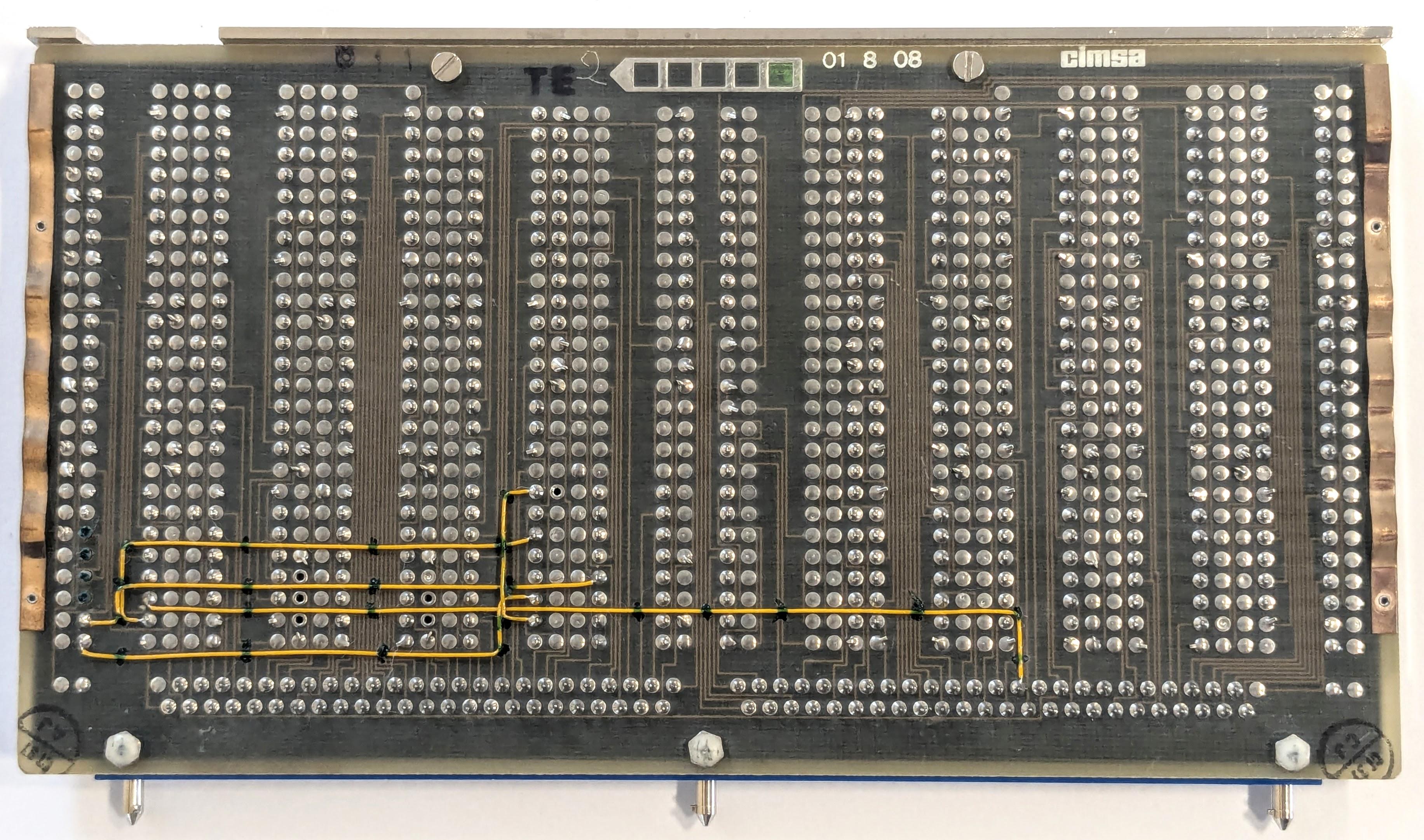
by kens
5/24/2026 at 12:25:35 AM
That looks vaguely breadboardish tooby mmastrac
5/24/2026 at 12:40:01 AM
> The PCB construction is curious (which you say is multi-layer) - why use a grid of 0.1" holes?The claim is multi-layer, but I seriously doubt that. I suspect that these are two-layer boards.
And if that's the case, the pattern is most likely because the holes precede the etch. And possibly precede the copper deposition so that the copper deposition can coat the insides of the holes.
And the holes are in a regular pattern because CNC simply wasn't a thing yet. You probably had some fixed array of drill bits that were used to make the holes in a very strict fixed automation fashion.
by bsder
5/24/2026 at 12:51:32 AM
Why do you doubt that these are multi-layer boards? IBM was making four-layer boards exactly like these in 1964 for the System/360 (signals on the top and bottom layers, power and ground in the middle layers).by kens
5/24/2026 at 3:02:58 AM
IBM was using flip chip in their mainframes in the same timeframe, too. That doesn't mean usage was widespread. This was 1970-1975, after all.In addition, 2-layer has some big advantages over 4 layer for reliability (won't delaminate under launch vibration, for example)--which is an issue in aerospace.
And, to my eye, these boards simply don't look like the have 4 layers nor are the laid out like that: https://upload.wikimedia.org/wikipedia/commons/7/7a/Mitra_15...
Besides, even if it were 4 layers, the issue is still that drilling holes in a non-regular pattern simply wasn't something that could be done easily 1975.
by bsder
5/24/2026 at 4:18:58 AM
I don't want to be rude, but I am not following your argument here. a) The computer that I'm examining is from 1980, not 1970, so I don't know why you're changing the time period. b) I have the circuit boards in front of me. They have more than two layers. c) You linked to a photo of a completely different computer. d) Drilling PCB holes in a non-regular pattern was trivial in 1975 and how most PCBs were built. Look at the S-100 boards from the Altair 8800 (1974) or look at the Apple I circuit board (1976) for instance.by kens
5/24/2026 at 6:45:54 AM
I mean, if you have the boards, then you obviously have the definitive answer about layers. Can't argue that.As you point out, if they designed this thing in the late 1970s, there is no reason for those giant arrays of drill holes. PCB design was definitely past this point by then and it would have been a hideous waste of time drilling all that just to fill them all up with wave soldering. It also blocks your routing terribly.
However, I assumed that this was likely a port of something from much earlier given the enormous lead times that aerospace requires (especially in the 1970s). There is absolutely no good reason to leave those extra holes which can become an assembly mistake otherwise.
"The Mitra 125, sometimes called "Mitra 15M/125" succeeded the Mitra 15 in 1975" That is the design that got used for the Spacelab Metra 125 MS in 1980, right?
I presumed that this was a port of a board which was a port of a board which was a port of a board given that design was obsolete even in 1975 since they apparently switched to the AMD bit slice processors even that far back.
And looking at Altair 8800 boards, you can see that the landing pads were very much NOT trivial, and look like they might even be hand drilled given the poor registration. Excellon/Esterline machines were still not that common outside of very high volume in 1975. By the time the Apple II came online a couple years later, though, the Excellon drilling machines were pretty commonplace.
by bsder